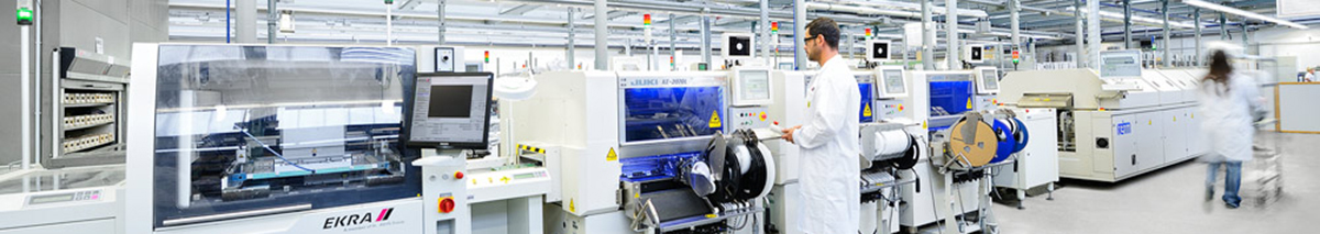
In the relentless pursuit of miniaturization and functionality, modern printed circuit board (PCB) design has evolved into a complex tapestry of mixed-technology components. While surface-mount technology (SMT) dominates, reliable through-hole (THT) connections remain critical for mechanical strength, high-power applications, and legacy components. This manufacturing duality presents a formidable challenge: how to efficiently and reliably solder these through-hole parts without damaging the surrounding, often delicate, surface-mount devices. The answer lies in the sophisticated world of advanced selective soldering equipment, a technology that has moved from a niche rework tool to a cornerstone of agile, high-quality electronics production.
The limitations of traditional wave soldering in this mixed-technology landscape are well-documented. The blanket application of a solder wave subjects the entire board bottom to high heat and solder contact, risking thermal damage to SMDs, creating unnecessary solder bridges, and leading to substantial material waste. Precision selective soldering systems elegantly solve this by targeting solder delivery only to the pre-defined through-hole areas that require it. This paradigm shift is powered by a synergy of innovative robotic automation, dynamic thermal management, and intelligent process control, offering manufacturers unprecedented flexibility and quality assurance.
At the core of a modern system is a high-speed, multi-axis programmable soldering robot. This robotic arm, equipped with a specialized solder nozzle or jet, follows exact paths uploaded from the board’s CAD data. The precision is remarkable, allowing for the soldering of connectors, pins, and terminals on densely populated boards with pin-to-pin spacing down to fractions of a millimeter. This robotic precision ensures consistent solder joint formation across every board in a batch, from the first to the thousandth, eliminating human error and variability.
However, precision movement alone is insufficient. The science of forming a perfect solder joint is governed by heat. This is where closed-loop thermal profiling and adaptive solder jet technology set new-generation equipment apart. Systems now feature real-time infrared or thermocouple feedback that monitors the temperature of the specific solder joint area during the process. The machine’s software dynamically adjusts the dwell time of the solder jet and the accompanying precise bottom-side preheating to ensure the board’s thermal mass reaches the ideal temperature for optimal solder flow and wetting. This prevents cold joints, lifts, and pad damage, especially on multilayer boards with significant thermal capacity.
The solder delivery system itself has seen radical innovation. Moving beyond simple dip-and-dwell methods, advanced systems employ laminar wave jets or micro-point nozzles. The laminar wave creates a stable, dross-free “curtain” of solder, perfect for drag-soldering rows of pins. Micro-point nozzles deliver tiny, targeted amounts of solder for individual joints. Crucially, these systems often operate in an inert nitrogen atmosphere within the soldering chamber. This nitrogen environment is a game-changer, drastically reducing oxidation to produce exceptionally bright, reliable solder joints with superior wetting characteristics and virtually zero solder balling or icicle formation.
The benefits of implementing such a flexible soldering cell extend far beyond joint quality. Dramatic solder and flux consumption reduction is a direct economic advantage, as material is applied only where needed, often leading to savings of 60-80% compared to a wave process. The focused heat application minimizes thermal stress across the entire assembly, preserving the integrity of adjacent SMT components like BGAs, QFNs, and delicate sensors. This significantly reduces downstream failure rates and field returns. Furthermore, the inherent flexibility of these systems makes them perfect for high-mix, low-volume (HMLV) production and rapid prototyping. Changeover between different board designs can be as simple as loading a new program, eliminating the need for costly and time-consuming pallet changes.
Integration into the smart factory is seamless. Modern selective soldering machines come equipped with sophisticated human-machine interface (HMI) panels and connectivity for Industry 4.0 data exchange. Production data, joint inspection logs (via optional integrated vision systems), maintenance alerts, and process parameters can be fed into a central Manufacturing Execution System (MES). This enables predictive process optimization, traceability for every soldered joint, and real-time production monitoring from anywhere in the world.
From automotive electronics control units (ECUs) laden with heavy connectors, to aerospace instrumentation requiring absolute reliability, to telecommunications infrastructure with its dense, high-layer-count boards, the applications are vast. As electronics continue to advance, with lead-free solder alloys requiring stricter process control and boards becoming ever more heterogeneous, the strategic importance of automated selective soldering technology will only grow. It is no longer just an alternative to wave soldering; it is the definitive solution for any manufacturer committed to zero-defect soldering, operational efficiency, and future-proofing their assembly lines.
Investing in a state-of-the-art selective soldering system is an investment in resilience, quality, and competitive edge. It transforms a challenging manufacturing bottleneck into a streamlined, reliable, and data-driven process, ensuring that the foundational connections within your products are as robust and precise as the innovative designs they enable.
Post time: Jan-19-2026


