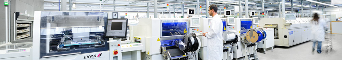
In the intricate ecosystem of electronics manufacturing, the reliability of through-hole connections remains paramount. Despite the proliferation of surface-mount technology, through-hole components continue to serve critical functions—providing mechanical strength for connectors, handling high power requirements in industrial applications, and accommodating legacy parts essential for specific designs. The challenge for manufacturers has always been how to efficiently solder these components at scale while maintaining impeccable quality. The answer has long been, and continues to evolve with, wave soldering technology, a process that has undergone remarkable transformation to meet the demands of modern electronics production.
Understanding the Wave Soldering Process Evolution
The fundamental principle of wave soldering—creating a standing wave of molten solder that contacts the underside of a PCB to form joints on through-hole components—has remained consistent for decades. However, the execution has evolved dramatically. Today’s advanced wave soldering machines represent a quantum leap from their predecessors, incorporating sophisticated controls, intelligent monitoring systems, and innovative design features that address the most persistent challenges in electronics assembly.
The journey of a PCB through a modern wave soldering system follows a carefully orchestrated sequence. It begins with precision flux application, where a thin, uniform layer of flux is applied to the board’s underside. This critical first step removes oxides from copper pads and component leads while promoting superior solder wetting. Contemporary systems offer multiple application methods, including spray fluxing with ultrasonic nozzle technology that produces an exceptionally fine, controlled mist, ensuring consistent coverage without excess that could lead to post-soldering residues.
Following flux application, the board enters the advanced preheating zone. This stage is far more sophisticated than simply raising temperature. Modern infrared and convection preheating modules work in concert to gradually elevate the PCB’s temperature, activating the flux and driving off solvents while preventing thermal shock to sensitive components. The preheating profile can be precisely tailored to each board’s specific thermal mass, with multiple independently controlled zones ensuring a smooth, controlled temperature ramp that eliminates warpage and delamination risks.
The Heart of the System: Solder Wave Dynamics
The soldering zone represents the culmination of the process, where the board meets the precision-controlled solder wave. Today’s wave soldering equipment features dual-wave configurations optimized for different board types. The initial turbulent wave, created by vibrating or oscillating mechanisms, ensures complete solder penetration into through-holes and around component leads, effectively eliminating shadowing effects where components block solder flow. This is followed by a smooth, laminar wave that removes excess solder, prevents bridging, and creates superior joint fillets with optimal contour.
The solder pot design itself has undergone significant refinement. Modern systems feature stainless steel construction with advanced heating elements that maintain temperature uniformity within ±1-2°C across the entire molten solder volume. This precision thermal management is essential for achieving consistent joint quality, particularly when working with lead-free alloys that require tighter process windows due to their higher melting points and different wetting characteristics.
Nitrogen Atmosphere: The Game-Changer in Wave Soldering
Perhaps the most significant advancement in recent years has been the integration of inert nitrogen atmospheres into wave soldering systems. Operating within a closed-loop nitrogen wave soldering environment transforms the process fundamentally. By flooding the soldering zone with nitrogen, oxygen levels are reduced to below 1000 ppm, dramatically limiting oxidation. The benefits cascade throughout the process: dross formation drops by up to 90%, drastically reducing solder consumption and maintenance requirements. Solder joints emerge with a brighter, shinier appearance that indicates superior metallurgical structure and enhanced reliability. Wetting improves noticeably, allowing for lower soldering temperatures and reduced thermal stress on boards and components. Perhaps most importantly for fine-pitch applications, solder balling and bridging are virtually eliminated, improving first-pass yields and reducing post-soldering inspection requirements.
Modern nitrogen-capable wave soldering systems incorporate sophisticated atmosphere management, with sensors continuously monitoring oxygen levels and adjusting nitrogen flow to maintain optimal conditions while minimizing consumption. The result is a cost-effective solution that delivers laboratory-quality joints in high-volume production environments.
Thermal Profiling Excellence
Achieving consistent results across diverse board types requires sophisticated thermal management capabilities. Contemporary wave soldering machines feature multi-zone precision thermal profiling that extends beyond simple temperature settings. These systems incorporate real-time feedback from sensors embedded throughout the process, allowing for dynamic adjustments that maintain optimal conditions despite variations in board thickness, copper weight, or component density.
The preheating system deserves particular attention. Modern configurations typically include 2-4 independently controlled zones, each utilizing a combination of quartz infrared emitters and forced convection. This hybrid approach ensures both rapid heat transfer and uniform temperature distribution across the entire board surface. The ability to create custom thermal profiles for each product family enables manufacturers to process sensitive assemblies without risk of thermal damage while maintaining the throughput required for cost-effective production.
Addressing Modern Manufacturing Challenges
Today’s electronics manufacturers face pressures that earlier generations could scarcely imagine. Component miniaturization continues unabated, with through-hole components now featuring lead spacings that approach those of fine-pitch SMT devices. Board densities have increased dramatically, with multiple layers and complex routing creating significant thermal management challenges. Meanwhile, quality expectations have never been higher, with industries such as automotive, medical, and aerospace demanding zero-defect soldering for mission-critical applications.
Advanced wave soldering solutions rise to these challenges through intelligent design. Adjustable conveyor systems with finger or palletized transport accommodate boards ranging from small modules to large backplanes. Programmable solder wave heights and adjustable nozzle configurations allow optimization for different component types and board geometries. Integrated fluxing systems with automatic density control ensure consistent application regardless of production volume or flux type.
For manufacturers dealing with mixed-technology boards—those combining through-hole components with surface-mount devices on the same assembly—modern wave soldering systems offer compatibility with protective pallets and fixtures. These precision-machined carriers shield SMD components from solder contact while exposing only the through-hole areas requiring soldering, enabling single-pass processing of complex assemblies that would otherwise require multiple operations.
Automation and Industry 4.0 Integration
The modern factory floor demands connectivity and intelligence from every piece of equipment. Contemporary wave soldering equipment delivers through comprehensive digital integration capabilities. Advanced control software with intuitive human-machine interface (HMI) provides operators with real-time visibility into every process parameter, from preheater temperatures to solder wave dynamics to conveyor speed.
Data collection and analysis capabilities enable unprecedented process optimization. Temperature profiles, flux application rates, nitrogen consumption, and production counts are automatically logged and can be exported for analysis or integrated with Manufacturing Execution Systems (MES) . This connectivity supports comprehensive traceability—essential for industries requiring documentation of every soldered joint’s process conditions—and enables predictive maintenance scheduling based on actual usage patterns rather than arbitrary time intervals.
The implementation of automated material handling interfaces further enhances productivity. Systems can communicate with upstream and downstream equipment, coordinating board flow to minimize wait times and maximize line efficiency. Recipe management capabilities allow instant changeover between products, storing thousands of profiles for immediate recall and eliminating setup errors.
Operational Efficiency and Cost Management
Beyond quality improvements, modern wave soldering technology delivers compelling economic benefits. Significant solder consumption reduction through nitrogen atmosphere implementation and optimized wave dynamics can reduce material costs by thousands of dollars annually. Minimized flux usage from precision application systems not only lowers consumable costs but also reduces post-soldering cleaning requirements and associated environmental impacts.
Energy efficiency has become a focal point in equipment design. Advanced insulation, high-efficiency heating elements, and intelligent power management systems reduce electricity consumption during both production and idle periods. Some systems incorporate standby modes that maintain process readiness while dramatically reducing power draw when boards are not being processed.
Environmental Responsibility and Compliance
As global regulations tighten around manufacturing processes, wave soldering technology has evolved to support environmentally responsible production. Lead-free soldering capability is now standard, with systems designed to handle the higher temperatures and different flow characteristics of lead-free alloys while maintaining joint quality. Efficient exhaust management systems capture and filter process emissions, ensuring a safe working environment and compliance with air quality regulations.
The dramatic reduction in dross generation through nitrogen atmosphere technology not only saves material costs but also reduces hazardous waste disposal requirements. Similarly, precision flux application minimizes volatile organic compound (VOC) emissions and reduces the environmental footprint of the soldering process.
Quality Assurance and Process Verification
Modern manufacturing demands proof of quality, not just the expectation of it. Advanced wave soldering systems incorporate features that support comprehensive quality assurance programs. Automatic solder pot level control ensures consistent wave height throughout production runs. Flux density monitoring verifies that application remains within specifications. Temperature verification systems with calibrated sensors confirm that thermal profiles match requirements for each board type.
For manufacturers requiring additional verification, optional in-line inspection systems can be integrated, providing real-time feedback on solder joint quality and enabling immediate process adjustments. This closed-loop quality control represents the ultimate expression of process optimization, catching potential issues before they result in defective products.
Applications Across Industries
The versatility of modern wave soldering technology makes it indispensable across diverse manufacturing sectors. In automotive electronics, where connectors must withstand vibration and thermal cycling for vehicle lifetimes, the reliable solder joints produced by advanced wave soldering ensure long-term dependability. Industrial control systems benefit from the ability to process heavy boards with large components while maintaining consistent quality. Consumer electronics manufacturers leverage the high throughput and low defect rates to meet demanding production schedules while controlling costs.
Telecommunications infrastructure, with its requirements for high-frequency performance and mechanical robustness, relies on wave soldering for connectors and shielding attachments. Power supply manufacturing depends on the process for soldering transformers, capacitors, and other high-mass components that SMT cannot accommodate. Medical device production demands the repeatable precision that only advanced automation can provide, ensuring that life-critical equipment performs flawlessly.
Future Directions in Wave Soldering Technology
As electronics manufacturing continues to evolve, so too will the wave soldering process. Emerging developments include enhanced artificial intelligence integration for predictive process optimization, where machine learning algorithms analyze production data to recommend parameter adjustments that improve yield. Advanced sensor technologies will provide even greater visibility into the soldering process, enabling real-time control at the individual joint level.
Sustainable manufacturing initiatives will drive further reductions in energy consumption and material waste. New solder alloy developments may require process adaptations, and wave soldering equipment will evolve to accommodate them. The integration of augmented reality for maintenance and troubleshooting will reduce downtime and enhance operator capabilities.
Conclusion: The Strategic Advantage of Modern Wave Soldering
In the competitive landscape of electronics manufacturing, the choice of soldering technology directly impacts quality, cost, and capability. Modern wave soldering systems represent the culmination of decades of process refinement, combining fundamental principles with cutting-edge technology to deliver exceptional results. From precision flux application through advanced thermal profiling to nitrogen-enhanced soldering, every aspect of the process has been optimized for reliability, efficiency, and quality.
For manufacturers committed to excellence in through-hole assembly, investing in contemporary wave soldering technology provides a clear competitive advantage. The ability to process complex boards with high yields, the flexibility to handle diverse product mixes, and the intelligence to optimize processes continuously—these capabilities translate directly to improved profitability and customer satisfaction.
Whether your production focuses on high-volume consumer goods, mission-critical industrial electronics, or specialized medical devices, today’s wave soldering solutions offer the performance, reliability, and intelligence required to succeed in global markets. By embracing these advances, manufacturers position themselves at the forefront of electronics assembly technology, ready to meet the challenges of tomorrow’s designs with confidence and capability.
Post time: Mar-02-2026


