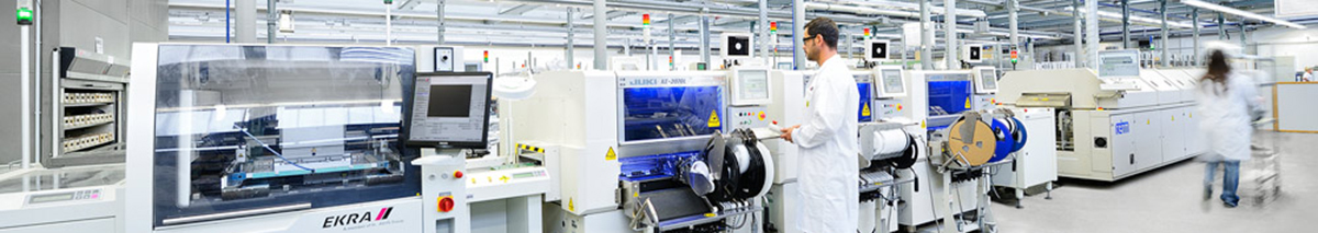
In the fast-evolving world of electronics manufacturing, precision, reliability, and throughput in PCB assembly are non-negotiable. Wave soldering remains a cornerstone technology for through-hole and mixed-technology board production, and its continued innovation is critical for businesses aiming to stay competitive. Today, we delve into the latest advancements in wave soldering equipment that are setting new benchmarks for quality and operational excellence.
Gone are the days of inconsistent solder joints and high defect rates. Modern wave soldering machines integrate sophisticated features designed to tackle the most complex assembly challenges. A key breakthrough is the advent of closed-loop nitrogen wave soldering systems. By injecting inert nitrogen into the soldering zone, these systems dramatically reduce oxidation on the solder wave and component leads. The result is exceptionally bright and reliable solder joints, virtually eliminating dross formation, improving wetting, and significantly reducing solder balling—a common headache in traditional setups.
Furthermore, precision thermal profiling has reached unprecedented levels. Advanced systems boast multi-zone, independently controlled preheating stages coupled with real-time monitoring. This ensures the PCB assembly undergoes a perfectly gradual and controlled temperature ramp, preventing thermal shock and ensuring all components reach the optimal temperature for solder flow. This meticulous control is paramount for preventing board warpage and delamination, especially when dealing with large or dense PCB assemblies.
Automation and smart technology are now at the heart of efficient production lines. The latest selective wave soldering technology deserves special attention. For boards requiring soldering only on specific areas—bypassing sensitive surface-mount devices (SMDs)—selective systems offer unparalleled precision. Utilizing programmable solder nozzles or miniature waves, they deliver targeted solder application. This not only conserves precious solder material but also protects nearby components from unnecessary heat exposure, making it ideal for high-mix, low-volume (HMLV) production and rework stations.
Beyond the soldering process itself, ergonomic design and sustainability are central to new equipment. Features like automatic flux density control, solder pot level maintenance, and integrated exhaust management systems contribute to a cleaner, safer, and more operator-friendly work environment. Moreover, enhanced energy recovery systems within the preheating and soldering zones reduce overall power consumption, aligning productivity gains with responsible manufacturing practices.
For manufacturers, the return on investment is clear: minimized rework, reduced consumption of solder and flux, lower defect rates, and increased line uptime. Whether you are producing automotive control units, industrial power supplies, consumer appliances, or telecommunications infrastructure, upgrading to a state-of-the-art wave soldering solution is a strategic move.
The future of electronics assembly demands flexibility and intelligence. The next generation of lead-free wave soldering equipment is already engineered to handle the specific requirements of environmentally compliant solder alloys with higher melting points. When integrated into a smart factory ecosystem, these machines provide valuable production data for predictive maintenance and process optimization, paving the way for Industry 4.0 readiness.
In conclusion, as circuit designs grow more complex and quality standards soar, leveraging advanced wave soldering technology is no longer an option but a necessity. It is the definitive step towards achieving flawless soldering results, remarkable cost savings, and superior end-product reliability in the global marketplace.
Post time: Jan-12-2026


