In the high-velocity world of electronics manufacturing, few processes are as critical—and as technically demanding—as reflow soldering. As surface-mount technology (SMT) continues its march toward ultra-miniaturization with components like 01005 passives and complex ball grid arrays (BGAs), the quality of the reflow process has become the single biggest determinant of long-term product reliability. While pick-and-place machines get the glory for speed, and inspection systems provide the checks, it is the reflow oven that silently, precisely, and conclusively forges the metallurgical bonds that bring a circuit board to life.
This comprehensive guide explores the intricate science behind modern reflow soldering technology. From the four critical thermal zones to the revolutionary impact of nitrogen atmospheres and vacuum-assist features, we examine how today’s thermal processing systems are tackling the most persistent defects in SMT assembly: tombstoning, voids, head-in-pillow defects, and excessive intermetallic growth. For any manufacturer seeking to transition from good soldering to world-class reliability, understanding these principles is non-negotiable.
Understanding Reflow Soldering: More Than Just Melting Solder
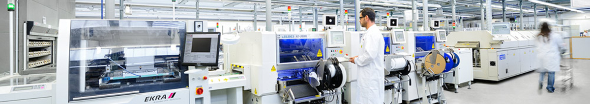
Reflow soldering is the dominant method for attaching surface-mount components to printed circuit boards (PCBs). Unlike wave soldering—which relies on a turbulent bath of molten solder—reflow utilizes solder paste, a precisely engineered suspension of solder alloy particles, flux, and binding agents. This paste is first applied to PCB pads via a stencil printing process. Components are then placed into the wet paste, which acts as a temporary adhesive. Finally, the entire assembly passes through a precisely controlled convection reflow oven, where a carefully orchestrated thermal profile melts the solder, activates the flux, and creates a permanent metallurgical bond.
The term “reflow” itself is descriptive: once the solder alloy solidifies below its melting point, it “flows back” to a liquid state when reheated above that critical temperature. However, the simplicity of this definition belies the extraordinary complexity of the physics, chemistry, and thermodynamics involved in producing a reliable joint at scale. Success requires balancing competing demands: heating must be fast enough for throughput but slow enough to prevent thermal shock; peak temperatures must be high enough to melt the alloy but low enough to protect sensitive components; and the time above liquidus (TAL) must be long enough for wetting but short enough to prevent excessive intermetallic compound growth.
The Four Essential Thermal Zones of a Reflow Profile
Every advanced reflow machine operates on a fundamental principle: controlled thermal transfer. The journey of a PCB through the oven is meticulously mapped by a thermal profile, represented as a graph of temperature versus time. While designs vary, all high-quality profiles are divided into four distinct zones, each serving a unique and non-negotiable purpose.
Zone 1: The Preheat Stage (Ambient to ~150°C)
The preheat zone is the gentle wake-up call for the PCB assembly. The primary objective here is to raise the temperature of the entire board safely and uniformly, typically at a rate of 1°C to 3°C per second . This controlled ramp is critical for several reasons. First, it gradually evaporates the volatile solvents within the solder paste binder. If the temperature rises too rapidly—exceeding 3°C/s—these solvents can boil violently, causing solder splatter or creating small, loose solder balls that can migrate and short adjacent pads.
Second, preheat minimizes thermal shock. A modern PCB is a heterogeneous assembly: a large, multi-layer BGA with a copper ground plane has vastly different thermal mass than a tiny 0402 ceramic capacitor. Rapid, uneven heating can induce catastrophic micro-cracks in Multi-Layer Ceramic Capacitors (MLCCs) due to the differential expansion rates between the ceramic body and its internal electrodes. Thus, preheat is the zone of risk mitigation, preparing the board for the intense heat to come without causing irreversible damage.
Zone 2: The Thermal Soak (150°C to ~180°C)
The soak, or dwell, zone is where thermal equilibrium is achieved. Lasting typically 60 to 120 seconds, this stage is deceptively simple: it stabilizes the temperature across the entire assembly, allowing cooler, massive components to “catch up” to smaller ones. By the end of this zone, the temperature delta across the entire PCB should be minimized, ideally near zero.
However, the soak stage is also where critical flux activation occurs. Solder paste contains mild organic acids designed to strip away oxides from the copper pads and component leads. For reliable wetting (the process of molten solder spreading across a clean metal surface), this oxide removal must happen before the solder melts. The soak temperature range is precisely calibrated to activate the flux without prematurely degrading it. If the soak is too short, residual oxides prevent wetting. If it is too long, the flux dries out and loses its cleaning power, leading to poor solder spreading or the dreaded “head-in-pillow” defect, where the BGA ball fails to coalesce with the paste.
Zone 3: The Reflow Zone (Above Liquidus)
This is the climax of the process—the reflow zone. In this stage, the oven’s temperature spikes to its peak value, typically 235°C to 250°C for lead-free SAC305 (Tin/Silver/Copper) alloys, which have a melting point (liquidus temperature) of approximately 217°C . The key parameter here is not just the peak temperature but the Time Above Liquidus (TAL) , which is typically held between 45 and 90 seconds.
Within this window, the physics of the soldering process transform. The individual solder powder particles in the paste coalesce into a single molten mass. The surface tension of this liquid metal creates self-alignment, a remarkable phenomenon where slightly misaligned components are physically pulled into correct position over their pads. Simultaneously, the flux residues, now fully activated, float to the surface.
Crucially, the molten solder reacts with the exposed copper pad to form a required Intermetallic Compound (IMC) layer, primarily Cu6Sn5. This microscopic layer (typically 1-5 µm thick) is the actual “glue” of the joint; it must be present for a good bond. However, the TAL must be strictly controlled. Too short a TAL results in a “cold solder joint”—dull, granular, and mechanically weak. Too long a TAL results in an excessively thick IMC layer (>5 µm), which becomes brittle and prone to fracture under mechanical stress . Managing this Goldilocks window is the central challenge of reflow engineering.
Zone 4: The Controlled Cooling Stage
The final zone is rapid, controlled cooling, typically targeting a rate of 2°C to 4°C per second . Fast cooling is desirable because it refines the grain structure of the solidifying solder, resulting in a joint with higher mechanical strength and fatigue resistance. Slow cooling allows large, brittle grains to form, weakening the joint. However, cooling too rapidly (e.g., quenching) can induce board warp due to Coefficient of Thermal Expansion (CTE) mismatches between the PCB substrate and the components. A controlled ramp is the signature of a high-quality industrial reflow oven.
Convection vs. Vapor Phase: Choosing Your Heat Transfer
The four-zone profile is the recipe, but the oven technology is the oven. The vast majority of today’s high-volume SMT lines utilize forced convection reflow ovens. These systems use high-velocity heated air or nitrogen jets to transfer heat to the PCB . Convection offers significant advantages: it is largely unaffected by component color or surface finish, reducing “shadowing” effects (where tall components block heat from smaller ones), and it provides excellent thermal uniformity across wide boards.
However, a niche but powerful alternative exists: Vapor Phase Soldering (VPS) . VPS uses the latent heat of vaporization of a special heat-transfer fluid. The board is lowered into a saturated vapor atmosphere, and the vapor condenses on the cooler PCB, releasing immense energy and instantly raising the board temperature to exactly the boiling point of the fluid (e.g., 230°C) . VPS offers theoretically perfect temperature uniformity and eliminates the risk of overheating, making it ideal for high-reliability applications like aerospace or for soldering thick, thermally massive boards where convection can struggle. The primary drawbacks are higher consumable fluid costs and slower throughput .
The Critical Role of Nitrogen Inert Atmosphere
In the pursuit of zero-defect soldering, the atmosphere inside the oven is just as important as the temperature. Standard air contains 21% oxygen, which aggressively reacts with molten solder at high temperatures, forming surface oxides that inhibit wetting and make joints look dull and gray.
This is why lead-free nitrogen reflow soldering ovens represent the gold standard for high-reliability manufacturing. By flooding the oven tunnel with inert Nitrogen (N2), the oxygen level is suppressed, typically to below 500 ppm (or even less than 50 ppm in advanced systems). The impact on quality is immediate and transformative: solder wetting angles improve, the flux requirement is reduced, and joints emerge bright and shiny, indicative of a healthy, oxide-free metallurgical structure.
The market recognizes this value. According to recent industry analysis, the global market for lead-free nitrogen reflow ovens was valued at approximately 495.3millionin2026andisprojectedtogrowatarobustCAGRof8.61 billion by 2034.This growth is driven by the increasing complexity of automotive electronics and IoT devices, where even a single defective joint can have catastrophic consequences. While nitrogen adds an operational cost, the reduction in dross, elimination of defects, and increased yield provide a rapid and compelling return on investment.
Vacuum Reflow: The Ultimate Void Elimination Solution
For the most demanding applications—power electronics, electric vehicle (EV) inverters, and medical implants—even microscopic voids in solder joints are unacceptable. Voids, pockets of trapped gas (often flux outgassing), act as thermal insulators, creating localized hot spots that degrade performance and lead to premature failure.
The solution is vacuum reflow soldering technology. High-end systems, such as the SRO i-LINE, integrate a vacuum chamber directly into the reflow process. After the PCB reaches peak temperature and the solder is molten, the chamber is evacuated to pressures below 1 mbar . This vacuum extracts trapped gases before the solder solidifies. The result is void-free solder joints with porosity often reduced to less than 1% – a dramatic improvement over standard convection methods. While historically used only for niche applications, vacuum reflow is rapidly becoming standard for SiC and GaN power devices in the booming EV market.
Tackling Advanced Packaging: Warpage Control and TrueFlat Technology
As the industry moves toward advanced semiconductor packaging, flip-chip bonding, and panel-level processing, a new challenge has emerged: board and substrate warpage. Ultra-thin PCBs (0.3 mm or less) and large panels are prone to warping during thermal cycling, leading to non-contact, open circuits, and “die tilt” (misalignment of semiconductor chips).
Innovative specialized reflow oven designs are addressing this head-on. The TrueFlat technology developed by industry leaders employs a recipe-controlled vacuum suction system embedded into the transport rails. As the PCB passes through the oven, gentle, uniform suction holds it perfectly flat against the conveyor, eliminating warpage in real time without requiring expensive new tooling or dedicated carriers . This capability maintains < 4°C thermal uniformity across panels up to 700mm x 700mm, enabling reliable, high-yield soldering for 2.5D/3D IC packaging and System-in-Package (SiP) modules. For high-density advanced SMT, eliminating chip tilt and ensuring coplanarity is no longer a luxury—it’s a requirement.
Process Control and Industry 4.0 Integration
Even the most advanced hardware is useless without intelligence. Modern SMT reflow equipment is fully integrated into the smart factory ecosystem. Features include:
- Closed-Loop Control: Real-time sensors continuously monitor temperature and conveyor speed, making micro-adjustments to maintain the exact profile.
- Recipe Management: Engineers can pre-load thousands of component-specific profiles for instant changeover.
- Connectivity: Standardized protocols (like IPC-CFX and GEM) allow the oven to communicate directly with MES (Manufacturing Execution Systems) and line controllers . Profile data, traceability logs, and alarm conditions are logged automatically.
- Predictive Maintenance: The system tracks its own health (blower RPMs, heater currents, conveyor wear) and alerts operators before a failure causes line stoppage.
Conclusion: The Strategic Value of Precision Reflow
In the competitive landscape of contract electronics manufacturing, the difference between winning and losing a contract often comes down to quality metrics—and reflow soldering is the heart of quality. A state-of-the-art reflow soldering furnace is not just a heater; it is a sophisticated thermal processing tool that integrates precision optics, fluid dynamics, metallurgy, and data science.
From the careful ramp of the preheat zone to the flux-cleaning action of the soak, the IMC-forming power of the reflow zone, and the grain-refining quench of cooling, every second inside the oven determines the reliability of the final product. By leveraging inert nitrogen atmospheres, vacuum void reduction, and advanced warpage control, manufacturers can consistently achieve the holy grail of SMT: zero defects.
For any operation serious about automotive, medical, aerospace, or high-end consumer electronics, investing in advanced reflow technology is a strategic imperative. It is the definitive path to achieving flawless solder joints, maximizing production yields, and building a reputation for unshakeable product quality in the global marketplace.
Reflow soldering is the dominant method for attaching surface-mount components to printed circuit boards(PCBs) . Unlike wave soldering-which relies on a turbulent bath of molten solder-reflow utilizes solder paste, a precisely enginerred suspension of solder alloy particles, flux, and binding agents. This paste is first applied to PCB pads via a stencil printing process. Components are then placed into the wet paste, which acts as a temporary adhesive. Finally, the entire assembly passes through a precisely controlled convection reflow oven, where a carefully orchestrated thermal profile melts the solder, activates the flux, and creates a permanent mentallurgical bond.
The term ”reflow” itself is descriptive: once the solder alloy solidifies below its melting point, it “floes back” to a liquid state when reheated above that critical temperature. However, the simplicity of this definition belies the extraordinary complexity of the physics, chemistry, and thermodynamics involved in producing a reliable joint at scale. Success requires balancing competing demands: heating must be fast enough for throughput but slow enough to prevent thermal shock; peak temperatures must be high enough to melt the alloy but low enough to protect sensitive components; and the time above liquidus (TAL) must be long enough for wetting but short enough to prevent excessive intermetallic compound growth.
Post time: May-05-2026


