Reflow soldering is the most widely used method of attaching surface mount components to printed circuit boards (PCBs). The aim of the process is to form acceptable solder joints by first pre-heating the components/PCB/solder paste and then melting the solder without causing damage by overheating.
The key aspects that lead to an effective reflow soldering process are as follows:
- Suitable machine
- Acceptable reflow profile
- PCB/component footprint Design
- Carefully printed PCB using well designed stencil
- Repeatable placement of surface mount components
- Good quality PCB, components and solder paste
Suitable Machine
There are various types of reflow soldering machine available depending on the required line speed and design/material of the PCB assemblies to be processed. The selected oven needs to be of a suitable size to handle the production rate of the pick and place equipment.
The line speed can be calculated as shown below:-
Line speed (minimum) = Boards per minute x Length per board
Load Factor (space between boards)
It is important to consider the repeatability of the process and so the ‘Load Factor’ is usually specified by the machine manufacturer, calculation shown below:

To be able to select the correct size reflow oven the process speed (defined below) must be greater than the minimum calculated line speed.
Process speed = Oven chamber heated length
Process dwell time
Below is an example of calculation to establish the correct oven size:-
An SMT assembler wants to produce 8-inch boards at a rate of 180 per hour. The solder paste manufacturer recommends a 4 minute, three step profile. How long an oven do I need to process boards at this throughput?
Boards per minute = 3 (180/hour)
Length per board = 8 inches
Load Factor = 0.8 (2-inch space between boards)
Process Dwell Time = 4 minutes
Calculate Line Speed: (3 boards/min) x (8 inches/board)
0.8
Line speed = 30 inches/minute
Therefore, the reflow oven must have a process speed of at least 30 inches per minute.
Determine oven chamber heated length with process speed equation:
30 in/min = Oven chamber heated length
4 minutes
Oven heated length = 120 inches (10 feet)
Note that the overall length of the oven will exceed 10 feet including the cooling section and conveyor loading sections. The calculation is for HEATED LENGTH – NOT OVERALL OVEN LENGTH.
1. Conveyor type – It is possible to select a machine with mesh conveyor but generally edge conveyors are specified to enable the oven to work in-line and be able to process double sided assemblies. In addition to the edge conveyor a centre-board-support is usually included to stop the PCB from sagging during the reflow process – see below. When processing double sided assemblies using the edge conveyor system care must be taken to not disturb components on the underside.

2. Closed loop control for speed of convection fans – There are certain surface mount packages such as the SOD323 (see insert) which have a small contact area to mass ratio which are susceptible to be disturbed during the reflow process. Closed loop speed control of the convention fans is a recommended option for assemblies using such parts.
3. Automatic control of conveyor and centre-board-support widths – Some machines have manual width adjustment but if there are many different assemblies to be processed with varying PCB widths then this option is recommended to maintain a consistent process.
Acceptable Reflow Profile
- Type of solder paste
- PCB material
- PCB thickness
- Number of layers
- Amount of copper within the PCB
- Number of surface mount components
- Type of surface mount components

In order to create a reflow profile thermocouples are connected to a sample assembly (usually with high temperature solder) in a number of locations to measure the range of temperatures across the PCB. It is recommended to have at least one thermocouple located on a pad towards the edge of the PCB and one thermocouple located on a pad towards the middle of the PCB. Ideally more thermocouples should be used to measure the full range of temperatures across the PCB – known as ‘Delta T’.
Within a typical reflow soldering profile there are usually four stages – Preheat, soak, reflow and cooling. The main aim being to transfer enough heat into the assembly to melt the solder and form the solder joints without causing any damage to components or PCB.
Preheat – During this phase the components, PCB and solder are all heated to a specified soak or dwell temperature being careful not to heat too quickly (usually no more than 2ºC/second – check solder paste datasheet). Heating too quickly can cause defects such as components to crack and the solder paste to splatter causing solder balls during reflow.

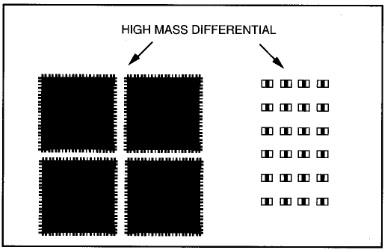
Soak – The purpose of this phase is to ensure all components are up to the required temperature before entering the reflow stage. Soak usually lasts for between 60 and 120 seconds depending on the ‘mass differential’ of the assembly and types of components present. The more efficient the heat transfer during the soak phase the less time is needed.

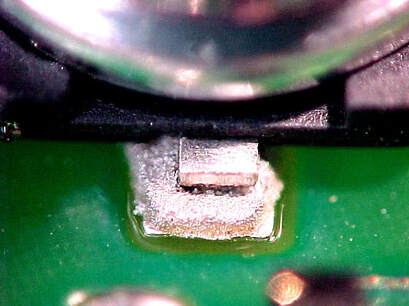
solder not formed fillet with lead
|
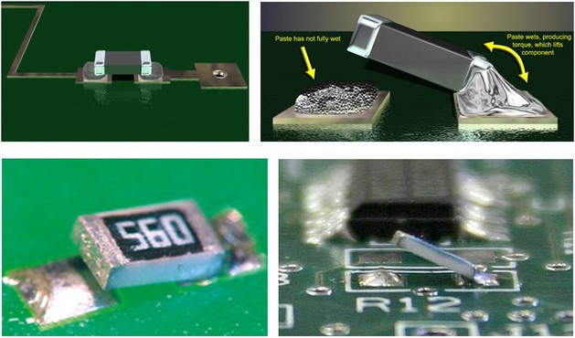
Not all solder balls melted
|
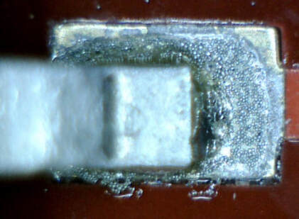
A common soldering defect after reflow is the formation of mid-chip solder balls/beads as can be seen below. The solution to this defect is to modify the stencil design - more details can be seen here.
|
|
Cooling – This is simply the stage during which the assembly is cooled but it is important to not cool the assembly too rapidly – usually the recommended rate of cooling should not exceed 3ºC/second.
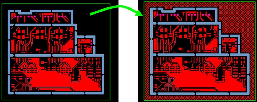
PCB/Component Footprint Design
|
|
Carefully printed PCB using well designed stencil
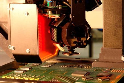
Repeatable placement of surface mount components
|

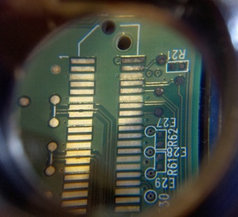
Component placement variation
|
Component placement programs can be created using the pick and place machines but this process isn’t as accurate as taking the centroid information directly from the PCB Gerber data. Quite often this centroid data is exported from the PCB design software but sometime is not available and so the service to generate the centroid file from Gerber data is offered by Surface Mount Process.
All components placement machines will have a ‘Placement Accuracy’ specified such as:-
35um (QFPs) to 60um (chips) @ 3 sigma
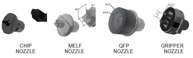
It is also important for the correct nozzle to be selected for the component type to be placed – a range of different component placement nozzles can be seen below:-
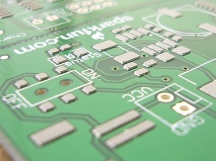
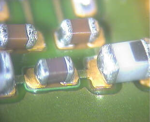
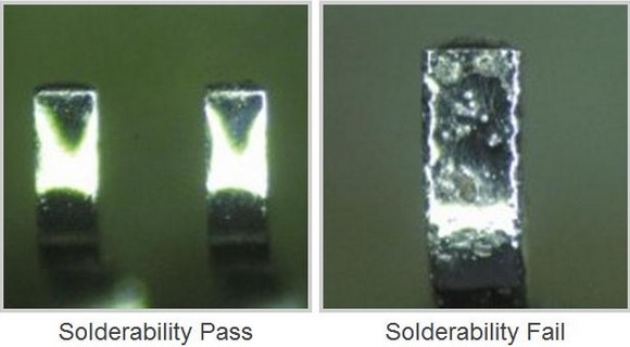
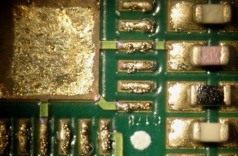
Good quality PCB, components and solder paste
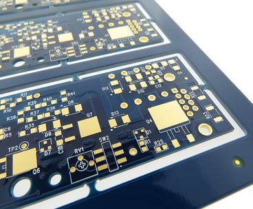
GOOD QUALITY PCB FINISH
|
TARNISHED PCB
|
Solder flowing to component and not PCB
|
Post time: Jun-14-2022


